
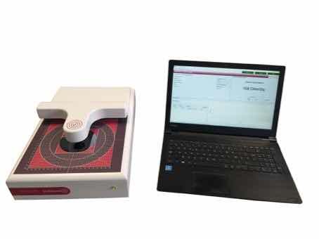

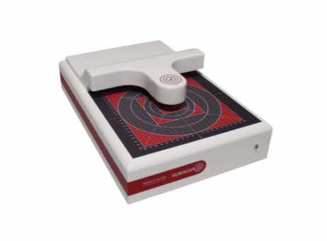

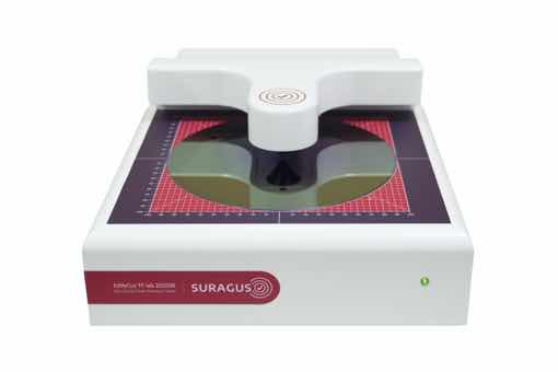


TF portableHandheld Eddy Current tester
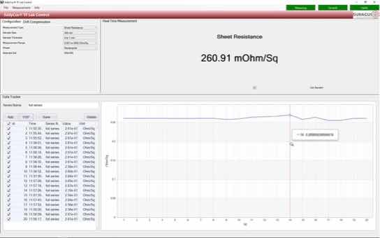
The portable TF 1010 system is a compact and portable measuring device for resistivity measurement over large areas. It allows the characterization by rapid contact of large conductive surfaces. The system uses the eddy current method. This method allows for non-destructive measurements. It is possible to measure encapsulated samples and components thanks to these weak currents which penetrate non-conductive layers such as oxides or any other coatings. The TF Portable 1010 is an easy-to-use device controlled via a touch screen. Compact, it allows, depending on its configuration, to precisely extract the surface resistance, the resistivity, the thickness or even the anisotropy of a material.
Advantages:
- Small and portable measurement device
- Manual measurement
- Instant live measurement
- Digital data collection and data transmission via Bluetooth
- Characterization of hidden and encapsulated conductive layers
Application:
- Architectural Glass (LowE)
- Mirror coatings
- Reflective layers
- Packaging foils
- Electrode layers in smart / electrochromic glass and energy storage
- Battery electrodes
- Conductive paper and conductive textiles
- Conductor Polymers
