


TF labManual Eddy Current tester
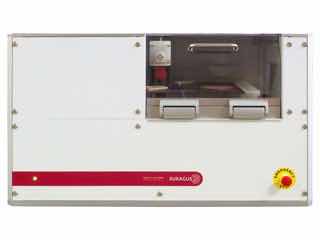
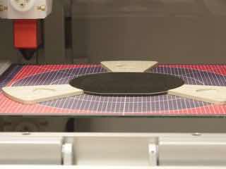
The EddyCus® lab 2020 SR Series is a compact, benchtop system designed for non-contact, single-point measurements of conductive thin films, metal layer thicknesses, and sheet resistance using eddy current technology. It enables fast, accurate measurements of samples up to 200 x 200 mm² (8 x 8 inches) and supports a broad range of materials, including thin metal layers, doped wafers, and conductive polymers.
The EddyCus® lab 2020 offers a modern, contact-free alternative to traditional 4-point probe (4PP) and other contact-based measurement methods. Unlike 4PP systems, it requires no physical contact, no surface preparation, and is unaffected by encapsulations or surface roughness. You can learn more about the comparison between eddy current and 4PP methods.
These advantages make the EddyCus® lab 2020 an excellent choice for R&D laboratories, quality control, and process monitoring, where speed, repeatability, and non-destructive testing are essential.
The EddyCus® lab 2020, which exists in several versions, allows measurements of:
- Surface resistance
- Resistivity
- Metal layer thickness
- Conductivity
- Anisotropy
- Emissivity
Advantage:
- Non destructive measurement
- Ultra-fast non-contact real-time measurement
- Accurate measurement of conductive thin layers at different penetration depths
- Characterization of hidden and encapsulated conductive layers
- Easy to use software & display of results in real time
Applications:
- Display, touch screen and flat screen
- OLED and LED applications
- Graphene layers
- Wafer and photovoltaic cells
- Semiconductor wafer
- Metallization layer and wafer metallization
- Battery electrodes
- Paper and textile conductors
- Organic conductor
- Polymer
- Coated architectural glass
- Smart electrochromic glass, Smart Glass
