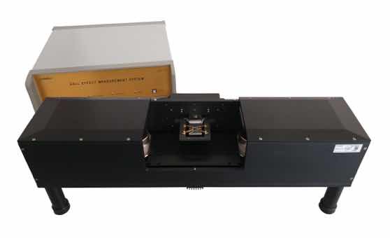
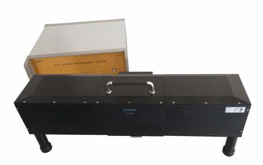
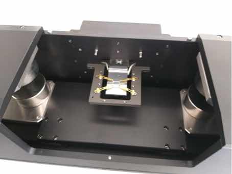
HMS5300      Semi-automatic Hall Effect measurement system for high temperatures

HMS5300 : Semi-automatic Hall Effect measurement system for high temperatures HMS5300 : Semi-automatic Hall Effect measurement system for high temperatures

Part Number

HMS5300

Designation

Semi-automatic Hall Effect measurement system for high temperatures

Description

The HMS5300 model is a compact tabletop system that uses the Van Der Pauw method to extract a number of internal parameters from samples of varying composition and geometry.
Compatible with temperature measurements ranging from 77K to 570K, this equipment makes it possible to characterize the resistivity, mobility, charge carrier density, Hall coefficient of a wide range of thin semiconductor layers.
The HMS5300 includes software capable of checking the quality of ohmic contacts by plotting I-V curves

Characteristic:

- Sample size: 5x5mm - 30x30mm
- Fixed magnet: 0.55T
- Temperature Measurement
- Current range: 1nA - 20mA

Compatibles temperature modules:

- AMP55T-RTSK: Ambient or 77K
- AMP55T-SH80350R: From 77K to 350K
- AHT55T3: From 300K to 570K

Applications:

- Si, Ge, SiGe, SiC, GaAs, InGaAs, InP, GaN, ZnO, TCOs
- Optoelectronic component - Nanomaterials
- Sensors, MEMS - Conductive polymer
- Oxide deposit
- Ceramic & Glass
- Batteries
- Electrodes
- Photovoltaic

MOST POPULAR REFERENCES

  • HMS5300-AMP55T-RTSK : For ambient temperature and 77K
  • HMS5300-AMP55T-SH80350K : With variable temperature module from 77K to 350K
  • HMS5300-AHT55T3 : With variable temperature module from 300K to 570K
  • HMS5300-AMP55T-AHT55T3 : With variable temperature modules from 77K to 350K and 300K to 570K

DOCUMENTS

Technical Specifications

Sample size

5x5 to 25x25 mm

Maximum sample thickness

2.5 mm

Magnet power

0.5 T

Magnet type

Permanent

Magnet material

Neodym

Magnet diameter

50 mm

Magnet movement

Automatic

Temperature range

77K to 570K, upon model

SMU

Internal

Current range

1nA to 20mA

Resistivity range

10E-4 to 10E7 ohm.cm

Concentration range

10E7 to 10E21 cm-3

Mobility range

1 to 10E7 cm2/Vs

Software

Yes (Windows)

License

Multi-users

IV curves

Yes

Parameters calculation

R, Res, Mob, Concentration, Hall

Temperature ramp

Yes

Data export

CSV

Computer

Not included (optional)

Electrical requirements

230VAC - 50Hz - Mono - 1A

Associated products

Sample holder for HMS series

SPCBSample holder for HMS series

These easy probe holders are composed of a small pcb on which the sample under test is held using spring clips.
The sample to measure is square with a pretty small size.


- Four individually adjustable gold plated spring needles allow a good electrical contact on each corner (may need a point of Indium solder deposited for better contact, not always necessary, depends on sample material).
- No soldering necessary
Semi-automatic Hall Effect measurement system with temperature

HMS5000Semi-automatic Hall Effect measurement system with temperature

The HMS5000 model is a compact tabletop system that uses the Van Der Pauw method to extract a number of internal parameters from samples of varying composition and geometry.
Compatible with temperature measurements ranging from 77K to 350K, this equipment makes it possible to characterize the resistivity, mobility, charge carrier density, Hall coefficient of a wide range of thin semiconductor layers.
The HMS5000 includes software capable of checking the quality of ohmic contacts by plotting I-V curves.

Characteristic:

- Sample size: 5x5mm - 30x30mm
- Fixed magnet: 0.55T
- Measurement in cold temperature
- Current range: 1nA - 20mA

Compatibles temperature modules:

- AMP55T-RTSK: Ambient or 77K
- AMP55T-SH80350R: From 77K to 350K

Applications:

- Si, Ge, SiGe, SiC, GaAs, InGaAs, InP, GaN, ZnO, TCOs
- Optoelectronic component
- Nanomaterials - Sensors, MEMS
- Conductive polymer
- Oxide deposit
- Ceramic & Glass
- Batteries
- Electrodes
- Photovoltaic
Semi-automatic Hall Effect measurement system for very high temperatures

HMS5500Semi-automatic Hall Effect measurement system for very high temperatures

The HMS5500 model is a compact tabletop system that uses the Van Der Pauw method to extract a number of internal parameters from samples of varying composition and geometry.
Compatible with temperature measurements ranging from 77K to 770K, this equipment makes it possible to characterize the resistivity, mobility, charge carrier density, Hall coefficient of a wide range of thin semiconductor layers.
The HMS5500 includes software capable of checking the quality of ohmic contacts by plotting I-V curves.

Characteristics:

- Sample size: 5x5mm - 30x30mm
- Fixed magnet: 0.55T
- Temperature Measurement
- Current range: 1nA - 20mA

Compatibles temperature modules:

- AMP55T-RTSK: Ambient or 77K
- AMP55T-SH80350R: From 77K to 350K
- AHT55T3: From 300K to 570K
- AHT55T5: From 300K to 770K

Applications:

- Si, Ge, SiGe, SiC, GaAs, InGaAs, InP, GaN, ZnO, TCOs
- Optoelectronic component - Nanomaterials
- Sensors, MEMS - Conductive polymer
- Oxide deposit
- Ceramic & Glass
- Batteries
- Electrodes
- Photovoltaic
Photonic Hall Effect measurement system

HMS7000Photonic Hall Effect measurement system

The HMS7000 Photonics will this time use the Van Der Pauw method under illumination to measure the response of several internal parameters of the material under different photonic stresses. This equipment is perfectly suited to the world of photovoltaics and the study of photoelectric semiconductors.

As for the other HMS series, it will characterize:

• Mobility of charge carriers
• Density of majority carriers
• The type of doping (P/N)
• Hall Voltage / Hall Coefficient
• Surface resistances, resistivity

Specifications:

• Fixed magnet: 0.51T
• "Visible illumination" photonic module (LED R,G,B)
• External source adapter (UV, IR)

Applications:

- Si, Ge, SiGe, SiC, GaAs, InGaAs, InP, GaN, ZnO, TCOs
- Optoelectronic component
- Nanomaterials
- Sensors, MEMS
- Conductive polymer
- Oxide deposit
- Ceramic & Glass
- Batteries
- Electrodes -
Photovoltaic
For technical and commercial information, quote, ordering or request of visit by our representative.
+33 (0)476 561 617

5 rue de la Verrerie

38120 Le Fontanil-Cornillon

Grenoble / France

Fax : +33(0) 476 757 484

RCS Grenoble B 381 001 171 - APE 4652Z

TVA FR 48 381 001 171