SPCB      Sample holder for HMS series

SPCB : Sample holder for HMS series SPCB : Sample holder for HMS series

Part Number

SPCB

Designation

Sample holder for HMS series

Description

These easy probe holders are composed of a small pcb on which the sample under test is held using spring clips.
The sample to measure is square with a pretty small size.


- Four individually adjustable gold plated spring needles allow a good electrical contact on each corner (may need a point of Indium solder deposited for better contact, not always necessary, depends on sample material).
- No soldering necessary

MOST POPULAR REFERENCES

  • SPCB-01 : For 5 x 5 mm to 20 x 20 mm sample, < 2 mm thickness
  • SPCB-11 : For 15 x 15 mm to 30 x 30 mm sample, < 2 mm thickness
  • SPCB-21 : For 5 x 5 mm to 20 x 20 mm sample, < 2 mm thickness (HMS5000 only)

Technical Specifications

Sample size

5x5 to 25x25 (65x65 on HMS3000 serie) mm

Thickness

Max 5.5 mm

Contact type

4 gold plated pogo pins

Temperature

No

Compatibility

HMS3000, HMS5X00/RTSK, HMS7000/RTSK

Associated products

Manual Hall Effect measurement system

HMS3000Manual Hall Effect measurement system

Discover our HMS3000 manual Hall effect system, designed for studying and characterizing the electrical properties of semiconductor materials and thin films. This educational and experimental equipment allows for the precise analysis of charge carrier mobility, carrier concentration, and resistivity of samples.

By measuring the voltages generated by Lorentz forces via its permanent magnet module, the system provides a concrete understanding of electronic transport phenomena and the effects of material doping. Compatible with the Van der Pauw method, it enables reliable measurements on various geometries and thin films.

Robust and easy to use, this manual Hall effect system is ideal for higher education laboratories, research centers, and characterization applications in semiconductor physics and materials science.

It is thus possible to calculate:

• Charge carrier mobility
• Majority carrier density (dopants)
• Doping type (P/N ratio)
• Hall voltage / Hall coefficient
• Surface resistances, resistivity, conductivity

Features:

• Sample size: 5x5 mm to 20x20 mm
• Measurement at two temperatures: ambient and 77 K
• Single or double magnet
• LN2 chamber
• ITO reference sample
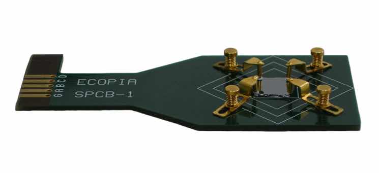
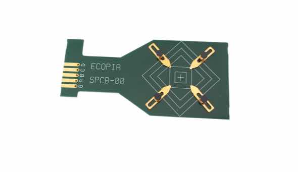
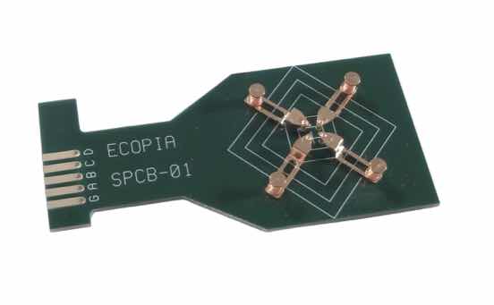
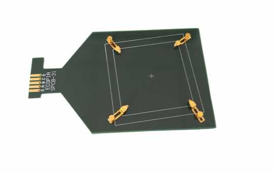
• Different SPCB sample holders depending on the application

Applications:

- Si, Ge, SiGe, SiC, GaAs, InGaAs, InP, GaN, ZnO, TCOs
- Optoelectronic component
- Nanomaterials - Sensors, MEMS
- Conductive polymer
- Oxide deposit
- Ceramic & Glass
- Batteries
- Electrodes
- Photovoltaic
Semi-automatic Hall Effect measurement system with temperature

HMS5000Semi-automatic Hall Effect measurement system with temperature

The HMS5000 is a motorized Hall effect measurement system dedicated to the electrical characterization of semiconductor materials using the Van der Pauw method. Designed to accommodate samples of varying compositions and geometries, it enables the precise extraction of numerous essential electrical parameters.
Compatible with temperature measurements from 77 K to 350 K, the HMS5000 offers a complete solution for the analysis of semiconductor thin films.

Thanks to its versatility, the system is suitable for both research activities and development and quality control applications in the fields of advanced materials and microelectronics.

The HMS5000 also integrates dedicated software that verifies the quality of ohmic contacts through the automatic plotting of I-V curves, thus ensuring the reliability and reproducibility of measurements. It also allows for the management of magnet movement and temperature ramps to plot the response of your sample.

It is therefore possible to calculate:

• Charge carrier mobility
• Majority carrier density (dopants)
• Doping type (P/N ratio)
• Hall voltage / Hall coefficient
• Surface resistance, resistivity, conductivity

Features:

• Sample size: 5x5mm - 20x20mm
Motorized dual magnets: 0.5T
Measurement under temperature: 77K to 350K
Current range: 1nA - 20mA

Applications:

- Si, Ge, SiGe, SiC, GaAs, InGaAs, InP, GaN, ZnO, TCOs
- Optoelectronic component
- Nanomaterials - Sensors, MEMS
- Conductive polymer
- Oxide deposit
- Ceramic & Glass
- Batteries
- Electrodes
- Photovoltaic
Semi-automatic Hall Effect measurement system for high temperatures

HMS5300Semi-automatic Hall Effect measurement system for high temperatures

Discover our HMS5300 semi-automatic Hall effect system, designed for studying and characterizing the electrical properties of semiconductor materials and thin films at varying temperatures. This educational and experimental equipment allows for the precise analysis of charge carrier mobility, carrier concentration, and sample resistivity.

By measuring the voltages generated under the influence of Lorentz forces via its permanent magnet module, the system provides a concrete understanding of electronic transport phenomena and the effects of material doping. Compatible with the Van der Pauw method, it enables reliable measurements on various geometries and thin films.

Robust and easy to use, this manual Hall effect system is ideal for higher education laboratories, research centers, and characterization applications in semiconductor physics and materials science.

Its semi-automatic temperature ramp system and magnetic field measurements make it completely autonomous during the measurement process.

It is therefore possible to calculate:

• Charge carrier mobility
• Majority carrier density (dopants)
• Doping type (P/N ratio)
• Hall voltage / Hall coefficient
• Surface resistance, resistivity, conductivity

Features:

• Sample size: 5x5mm - 20x20mm
• Motorized dual magnets: 0.5T
• Measurement under temperature: 77K to 350K
• Current range: 1nA - 20mA

Compatibles temperature modules:

- AMP55T-RTSK: Ambient or 77K
- AMP55T-SH80350K: From 77K to 350K
- AHT55T3: From 300K to 570K
- AHT55T5: From 300K to 770K

Applications:

- Si, Ge, SiGe, SiC, GaAs, InGaAs, InP, GaN, ZnO, TCOs
- Optoelectronic component - Nanomaterials
- Sensors, MEMS - Conductive polymer
- Oxide deposit
- Ceramic & Glass
- Batteries
- Electrodes
- Photovoltaic
Semi-automatic Hall Effect measurement system for very high temperatures

HMS5500Semi-automatic Hall Effect measurement system for very high temperatures

Discover our HMS5500 semi-automatic Hall effect system, designed for studying and characterizing the electrical properties of semiconductor materials and thin films at varying temperatures. This educational and experimental equipment allows for the precise analysis of charge carrier mobility, carrier concentration, and sample resistivity.

By measuring the voltages generated under the influence of Lorentz forces via its permanent magnet module, the system provides a concrete understanding of electronic transport phenomena and the effects of material doping. Compatible with the Van der Pauw method, it enables reliable measurements on various geometries and thin films.

Robust and easy to use, this manual Hall effect system is ideal for higher education laboratories, research centers, and characterization applications in semiconductor physics and materials science.

Its semi-automatic temperature ramp system and magnetic field measurements make it completely autonomous during the measurement process.

It is therefore possible to calculate:

• Charge carrier mobility
• Majority carrier density (dopants)
• Doping type (P/N ratio)
• Hall voltage / Hall coefficient
• Surface resistance, resistivity, conductivity

Features:

• Sample size: 5x5mm - 20x20mm
• Motorized dual magnets: 0.5T
• Measurement under temperature: 77K to 350K
• Current range: 1nA - 20mA


Compatibles temperature modules:

- AMP55T-RTSK: Ambient or 77K
- AMP55T-SH80350K: From 77K to 350K
- AHT55T3: From 300K to 570K
- AHT55T5: From 300K to 770K

Applications:

- Si, Ge, SiGe, SiC, GaAs, InGaAs, InP, GaN, ZnO, TCOs
- Optoelectronic component - Nanomaterials
- Sensors, MEMS - Conductive polymer
- Oxide deposit
- Ceramic & Glass
- Batteries
- Electrodes
- Photovoltaic
Photonic Hall Effect measurement system

HMS7000Photonic Hall Effect measurement system

The HMS7000 Photonics will this time use the Van Der Pauw method under illumination to measure the response of several internal parameters of the material under different photonic stresses. This equipment is perfectly suited to the world of photovoltaics and the study of photoelectric semiconductors.

As for the other HMS series, it will characterize:

• Mobility of charge carriers
• Density of majority carriers
• The type of doping (P/N)
• Hall Voltage / Hall Coefficient
• Surface resistances, resistivity

Specifications:

• Fixed magnet: 0.51T
• "Visible illumination" photonic module (LED R,G,B)
• External source adapter (UV, IR)

Applications:

- Si, Ge, SiGe, SiC, GaAs, InGaAs, InP, GaN, ZnO, TCOs
- Optoelectronic component
- Nanomaterials
- Sensors, MEMS
- Conductive polymer
- Oxide deposit
- Ceramic & Glass
- Batteries
- Electrodes -
Photovoltaic
For technical and commercial information, quote, ordering or request of visit by our representative.
+33 (0)476 561 617

5 rue de la Verrerie

38120 Le Fontanil-Cornillon

Grenoble / France

Fax : +33(0) 476 757 484

RCS Grenoble B 381 001 171 - APE 4652Z

TVA FR 48 381 001 171