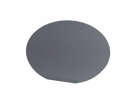
SRS3      Calibration wafer NIST certified

SRS3 : Calibration wafer NIST certified SRS3 : Calibration wafer NIST certified

Part Number

SRS3

Designation

Calibration wafer NIST certified

Description

This wafer is used to calibrate 4-point resistivity measurement systems. It has NIST certification.

Specifications:

• 3" (75mm) wafer
• NIST certification during 1 year

MOST POPULAR REFERENCES

  • SRS3-0.002 : Resistivity of 0.002 ohm.cm
  • SRS3-0.01 : Resisitivity of 0.01 ohm.cm
  • SRS3-0.03 : Resistivity of 0.03 ohm.cm
  • SRS3-0.1 : Resistivity of 0.1 ohm.cm
  • SRS3-0.3 : Resistivity of 0.3 ohm.cm
  • SRS3-0.9 : Resistivity of 0.9 ohm.cm
  • SRS3-3 : Resistivity of 3 ohm.cm

DOCUMENTS

Technical Specifications

Sheet resistance range

0.002 to 3 Ohm.cm

Wafer size

76.2 mm

Material

Silicon

Thickness

508 µm

Site number

1

NIST certificate

Yes

Associated products

4 point probe manual measurement package medium resistivity range

MW-Pack4PP-M4 point probe manual measurement package medium resistivity range

Manual sheet resistivity measurement systems for laboratories, for research and small productions. The stand includes several features enabling it to measure resistivity and surface resistance using 4 precise points. It is possible to characterize materials manufactured by semiconductor doping, metal or glass deposition, rubber materials, etc.

A manual lever makes it possible to make a movement in Z of contact and non-contact with a repeatability of the order of a micron. In addition, an adjustment wheel located on the top of the device makes it possible to fine-tune the movement in Z with precision.
The sample to be tested is mounted on a mobile support which allows it to be easily placed under the measuring head between each measurement point.
In addition, the equipment has several chuck sizes ranging from 4" to 12".

Applications:

- Si, Ge, SiGe, SiC, GaAs, InGaAs, InP, GaN, ZnO, TCO
- Oxide deposit
-Sensors, MEMS
- Conductive polymer
- Batteries
- Electrodes
- Photovoltaic
- Ceramic & Glass
- Optoelectronic component
- Nanomaterials


Specifications:


• I/V measurement, sheet resistance, resistivity or thickness
• Cartography
• A micro-switch ensures the injection of current from the moment all the tips are in contact.
• The measurement is performed by an external Keithley 2450 device.
• Software for data processing
• Creation of an I/V curve
• Bipolar measurement
• Data export in Txt, Excel, CSV format...

The measurement system uses software for measurement and display of results that allows data export for later data processing. It is possible to map the sample according to the resistivities or thicknesses measured.
The user entered the size and shape of the sample, the exclusion edge and the number of points to be tested. A graphic image of the target measurement points is displayed. At the end of the test of all the points, we find the average of the measured values, the standard deviation as well as the maximum and minimum measurement.

4 point probe stand

S3024 point probe stand

The configuration is composed of a stand holding the probe head with a quick Z lever and a chuck for wafer of 4" or 6", the sample positioning is manual as well as the contact of the tips by a rotating lever.

Applications:

- Si, Ge, SiGe, SiC, GaAs, InGaAs, InP, GaN, ZnO, TCO
- Oxide deposit
-Sensors, MEMS
- Conductive polymer
- Batteries
- Electrodes
- Photovoltaic
- Ceramic & Glass
- Optoelectronic component
- Nanomaterials

Specifications:

• A micro-switch insures that the current will be injected only after contact of the 4-point probe head
• The  measurement itself is provided from an external sourcemeter and voltmeter typically Keithley family, which can be supplied if requested
• The system can be upgraded to include the measurement and display onto a PC
• Perfect tool for for laboratories, universities, research centers... in the material characterization.
Semi-automatic 4 point probe measurement under temperature

QUADPRO2ASemi-automatic 4 point probe measurement under temperature

Semi-automatic 4-point in-line temperature measurement system on samples ranging from 10mm to 300mm in diameter.. Capable of measuring surface resistance ranges from 10μΩ/sq to 10GΩ/sq. Several versions possibles to optimize measurement accuracy according to the ranges measured.

Equipment feature:

• V/I measurement, sheet resistance, resistivity or thickness
• Mean, Standard Deviation, Minimum, Maximum and 3Sigma reports for the dataset
• Temperature Coefficient of Resistance (TCR) measurements
• Automated 2D mapping, 3D mapping and cross-section
• Ultra high precision and repeatability
• Comparative mapping

The TCR option

The Resistance Temperature Coefficient option integrates sample temperature control as well as automated injected current control and resistance calculations. Integrated with a thermal chuck system, the test automatically sweeps temperatures over a wide range without moving the test tips.
Measurements are taken at each target temperature and the results are plotted on a graph. The TCR is expressed in parts per million (PPM). Users define the temperature range, steps, and delay for each test point before taking a measurement. A variety of thermal chucks are available to set the range and resolution from room temperature to 300°C, with 1° resolution.
Data can be printed or exported to a spreadsheet for further analysis.

8

280I8" semi-automatic 4 point probe measurement system

Semi-automatic 4-point in-line measurement systems on samples ranging from 10mm to 200mm in diameter. Thanks to their motorized chucks, the 280I can map up to 6000 measurement points on surface resistance ranges from 1 mohm/sq to 8E5 Ohm/sq.

Specification:

• Extended range down to 8E11 Ohm/sq.
• Different versions adapted to the different resistance ranges tested
• Several types of mapping: 1pts, 5pts, 9pts, diagonal, Cartesian, custom etc..
• Powerful calculation algorithm
• Edge effect compensation, geometric factor
• SEC II Communication


Application:

- Si, Ge, SiGe, SiC, GaAs, InGaAs, InP, GaN, ZnO, TCOs
- Optoelectronic component
- Nanomaterials
- Sensors, MEMS
- Conductive polymer
- Oxide deposit
- Ceramic & Glass
- Batteries
- Electrodes
- Photovoltaic

Manual 4 point probe measurement under temperature

QUADPRO2MManual 4 point probe measurement under temperature

4-point manual in-line temperature measurement system on samples ranging from 10mm to 300mm in diameter.. Capable of measuring surface resistance ranges from 10μΩ/sq to 10GΩ/sq. Several versions possibles to optimize measurement accuracy according to the ranges measured.

Equipment feature:

• V/I measurement, sheet resistance, resistivity or thickness
• Mean, Standard Deviation, Minimum, Maximum and 3Sigma reports for the dataset
• Temperature Coefficient of Resistance (TCR) measurements
• Automated 2D mapping, 3D mapping and cross-section
• Ultra high precision and repeatability
• Comparative mapping

The TCR option

The Resistance Temperature Coefficient option integrates sample temperature control as well as automated injected current control and resistance calculations. Integrated with a thermal chuck system, the test automatically sweeps temperatures over a wide range without moving the test tips.
Measurements are taken at each target temperature and the results are plotted on a graph. The TCR is expressed in parts per million (PPM). Users define the temperature range, steps, and delay for each test point before taking a measurement. A variety of thermal chucks are available to set the range and resolution from room temperature to 300°C, with 1° resolution.
Data can be printed or exported to a spreadsheet for further analysis.
12

333A12" semi-automatic 4 point probe measurement system

Semi-automatic 4-point in-line measurement systems on samples ranging from 10mm to 200mm in diameter. Thanks to their motorized chucks, the 333A can map up to 6000 measurement points on surface resistance ranges from 1 mohm/sq to 8E11 Ohm/sq.

Specification:

• Different versions adapted to the different resistance ranges tested
• Several types of mapping: 1pts, 5pts, 9pts, diagonal, Cartesian, custom etc..
• Powerful calculation algorithm
• Edge effect compensation, geometric factor
• SECS II Communication
• Possible version in Full-Automatic with loading of wafers via cassette and pre-alignment


Application:

- Si, Ge, SiGe, SiC, GaAs, InGaAs, InP, GaN, ZnO, TCOs
- Optoelectronic component
- Nanomaterials
- Sensors, MEMS
- Conductive polymer
- Oxide deposit
- Ceramic & Glass
- Batteries
- Electrodes
- Photovoltaic

4 point probe manual measurement package high resisitivy range

MW-Pack4PP-H4 point probe manual measurement package high resisitivy range

Manual sheet resistivity measurement systems for laboratories, for research and small productions. The stand includes several features enabling it to measure resistivity and surface resistance using 4 precise points. It is possible to characterize materials manufactured by semiconductor doping, metal or glass deposition, rubber materials, etc.

A manual lever makes it possible to make a movement in Z of contact and non-contact with a repeatability of the order of a micron. In addition, an adjustment wheel located on the top of the device makes it possible to fine-tune the movement in Z with precision.
The sample to be tested is mounted on a mobile support which allows it to be easily placed under the measuring head between each measurement point.
In addition, the equipment has several chuck sizes ranging from 4" to 12".

Applications:

- Si, Ge, SiGe, SiC, GaAs, InGaAs, InP, GaN, ZnO, TCO
- Oxide deposit
-Sensors, MEMS
- Conductive polymer
- Batteries
- Electrodes
- Photovoltaic
- Ceramic & Glass
- Optoelectronic component
- Nanomaterials

Specifications:


• I/V measurement, sheet resistance, resistivity or thickness
• Software for data processing
• Creation of an I/V curve
• Bipolar measurement
• Data export in Txt, Excel, CSV format...
• A micro-switch ensures the injection of current from the moment all the tips are in contact.
• The measurement is performed by an external Keithley 2635B device.


The measurement system uses software for measurement and display of results that allows data export for later data processing. It is possible to map the sample according to the resistivities or thicknesses measured.
The user entered the size and shape of the sample, the exclusion edge and the number of points to be tested. A graphic image of the target measurement points is displayed. At the end of the test of all the points, we find the average of the measured values, the standard deviation as well as the maximum and minimum measurement.
4 point probe stand large area

S3034 point probe stand large area

The configuration is composed of a stand holding the probe head with a quick Z lever and a chuck for wafer of 8" or 12", the sample positioning is manual as well as the contact of the tips by a rotating lever.

Applications:

- Si, Ge, SiGe, SiC, GaAs, InGaAs, InP, GaN, ZnO, TCO
- Oxide deposit
-Sensors, MEMS
- Conductive polymer
- Batteries
- Electrodes
- Photovoltaic
- Ceramic & Glass
- Optoelectronic component
- Nanomaterials

Specifications:

• A micro-switch insures that the current will be injected only after contact of the 4-point probe head
• The  measurement itself is provided from an external sourcemeter and voltmeter typically Keithley family, which can be supplied if requested
• The system can be upgraded to include the measurement and display onto a PC
• Perfect tool for for laboratories, universities, research centers... in the material characterization.
For technical and commercial information, quote, ordering or request of visit by our representative.
+33 (0)476 561 617

5 rue de la Verrerie

38120 Le Fontanil-Cornillon

Grenoble / France

Fax : +33(0) 476 757 484

RCS Grenoble B 381 001 171 - APE 4652Z

TVA FR 48 381 001 171